mk1 C920 PCBA wiring
New C920 wiring
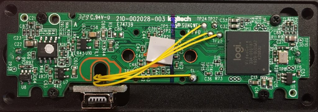
Recently updated C920 webcam version was released featuring new PCB. These changes introduced two unexpected issues: wiring is different and new PCB has mechanical interference with aluminium rework kit back plate.
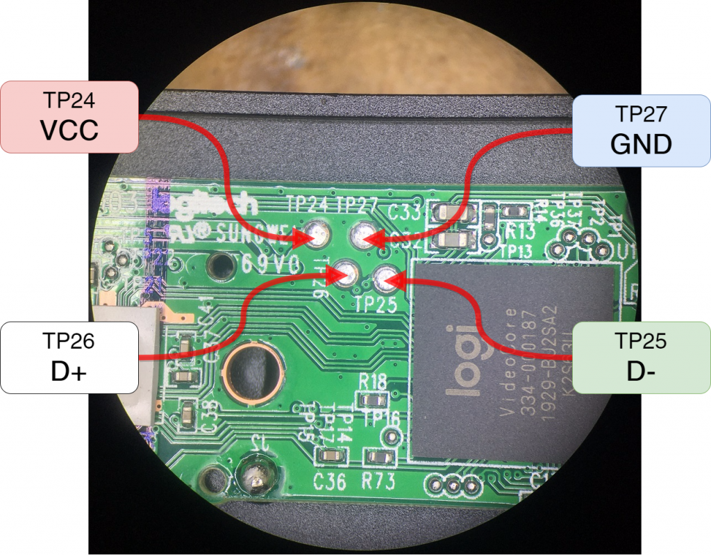
If you rework webcam by yourself, please use pin-out diagram as pictured below to solder wires.
| Test point | Signal |
| TP24 | VCC |
| TP26 | USB D+ |
| TP25 | USB D- |
| TP27 | GND |
Interesting note - looks like new PCB release was rushed, spot mirrored J2 designator.
Original blog post about changes
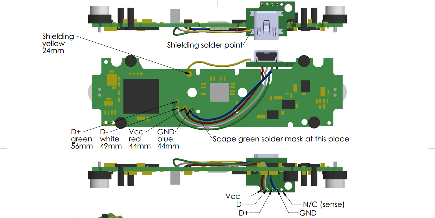
Old C920 wiring
Route USB wires as indicated in this diagram. I found Kynar monolithic wires are the best – small and easy to solder. 5 wires will be used USB D+, D-, GND, Power. Shield also has to be soldered.
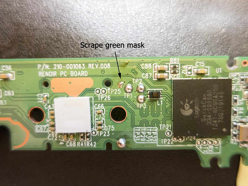
USB connector is available on the other side of PCB and it is surface mount type. Therefore it will be easier to use test pins. While GND is not available as test pin I recommend making pad by yourself. You can also use other places to solder GND wire, it is just my recommendation. Scrape green soldering mask with scalpel to access GND.


